TSMC co-COO says company is unafraid of Intel’s packaging technology challenge
Kevin Zhang addressed Intel's EMIB gains at TSMC's North America Technology Symposium, while revealing an aggressive roadmap to maintain dominance in AI chip packaging.
Share
Add us on Google by Editorial Team Jun. 4, 2026The semiconductor packaging war just got a new chapter. At TSMC’s North America Technology Symposium on April 22, 2026, Deputy Co-COO Kevin Zhang made it clear that the world’s largest contract chipmaker isn’t losing sleep over Intel’s advances in advanced packaging, even as major hyperscalers start exploring alternatives.
The confident posture comes at an interesting moment. Google has reportedly adopted Intel’s Embedded Multi-Die Interconnect Bridge (EMIB) technology for at least one project, choosing it over TSMC’s offerings due to advantages in reticle size. Amazon is also reportedly showing increased interest in Intel’s EMIB technology.
The packaging technology battle, explained
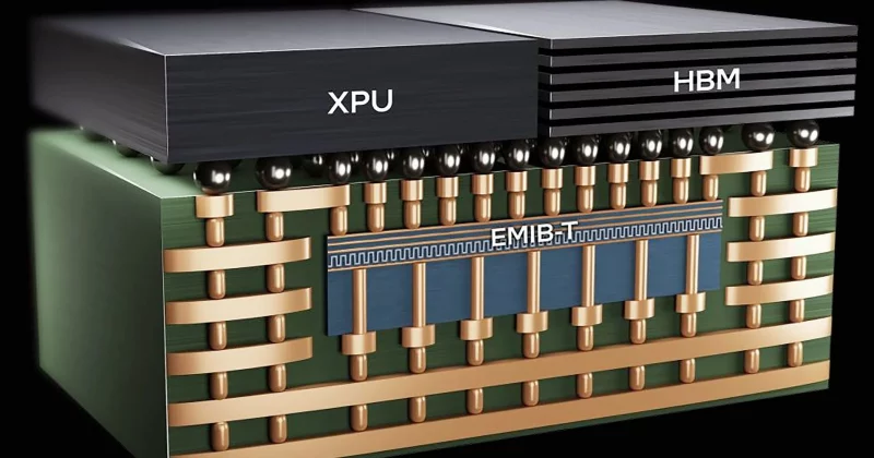
TSMC has built its packaging empire around a family of technologies called CoWoS, short for Chip-on-Wafer-on-Substrate. The CoWoS family includes several variants, CoWoS-S, CoWoS-R, and CoWoS-L, each optimized for different use cases. These technologies are the backbone of high-volume AI chip production, including NVIDIA’s GPUs that power the current AI infrastructure boom.
AdvertisementIntel’s counter-move is EMIB, which embeds small silicon bridges directly into organic substrates. It’s a 2.5D packaging solution that competes directly with CoWoS.
Zhang acknowledged Intel’s innovations during the symposium but framed them as alternatives that come with their own set of challenges.
Why Google’s EMIB adoption matters
Google reportedly chose EMIB because current CoWoS solutions can’t match its reticle-size advantages. For AI workloads that demand ever-larger silicon configurations, that ceiling matters enormously.
Zhang revealed that the company is accelerating its packaging roadmap, targeting a 14-reticle CoWoS version for release by 2028. If successful, it would effectively neutralize the reticle-size advantage that made EMIB attractive to Google in the first place.
What this means for investors
For TSMC, the CoWoS family remains its crown jewel in packaging. The technology is deeply embedded in NVIDIA’s GPU production pipeline. Intel’s EMIB gains are notable, but winning one Google project is different from displacing TSMC as the default packaging choice for the industry.
The 2028 timeline for TSMC’s 14-reticle CoWoS gives Intel a window to consolidate relationships with hyperscalers who need larger packaging solutions now. EMIB’s use of organic substrates rather than full silicon interposers could also offer cost advantages at scale.
Disclosure: This article was edited by Editorial Team. For more information on how we create and review content, see our Editorial Policy.